Question: Determine Zi, Zo, and Av for the
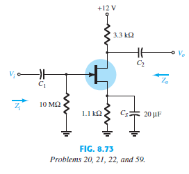
Determine Zi, Zo, and Av for the network of Fig. 8.73 if gfs = 3000 mS and gos = 50 ms.
> For the network of Fig. 9.79: a. Determine the mathematical expression for the magnitude of the ratio VO>VI. b. Using the results of part (a), determine Vo>Vi at 100 Hz, 1 kHz, 2 kHz, 5 kHz, and 10 kHz, and plot the resulting curve for the frequenc
> Given the characteristics of Fig. 9.78, sketch: a. The normalized gain. b. The normalized dB gain (and determine the bandwidth and cutoff frequencies). /
> a. Determine the common logarithm of the following numbers: 103, 50, and 0.707. b. Determine the natural logarithm of the numbers appearing in part (a). c. Compare the solutions of parts (a) and (b).
> For a JFET having specified values of gfs = 4.5 mS and gos = 25 mS, determine the device output impedance Zo (FET) and device ideal voltage gain Av(FET).
> A specification sheet provides the following data (at a listed drain-source current): / At the listed drain–source current, determine: a. gm. b. rd.
> Determine the value of gm for a JFET (IDSS = 8 mA, VP = - 5 V) when biased at VGSQ = VP>4.
> A JFET (IDSS = 10 mA, VP = - 5 V) is biased at ID = IDSS>4. What is the value of gm at that bias point?
> Determine the saturation current (ICsat) for the network of Fig. 4.125.
> Calculate the input impedance (Zi) and output impedance (Zo) for the amplifier circuit of Fig. 8.94.
> For the amplifier circuit of Fig. 8.94, calculate the voltage gain of each stage and the overall amplifier voltage gain.
> For the cascade amplifier of Fig. 8.94, calculate the dc bias voltages currents of each stage.
> For the cascade amplifier of Fig. 8.93, using JFETs with specifications IDSS = 12 mA, VP = - 3 V, and gos = 25 mS, calculate the circuit input impedance (Zi) and output impedance (Zo).
> If both JFETs in the cascade amplifier of Fig. 8.93 are changed to those having the specifications IDSS = 12 mA, VP = - 3 V, and gos = 25 mS, calculate the resulting voltage gain for each stage, the overall voltage gain, and the output voltage, Vo.
> If both JFETs in the cascade amplifier of Fig. 8.93 are changed to those having specifications IDSS = 12 mA and VP = - 3 V, calculate the resulting dc bias of each stage.
> For the JFET cascade amplifier of Fig. 8.93, using identical JFETs with IDSS = 8 mA and VP = - 4.5 V, calculate the voltage gain of each stage, the overall gain of the amplifier, and the output voltage Vo.
> For the JFET cascade amplifier in Fig. 8.93, calculate the dc bias conditions for the two identical stages, using JFETs with IDSS = 8 mA and VP = - 4.5 V.
> For a JFET having gm = 6 mS at VGSQ = - 1 V, what is the value of IDSS if VP = - 2.5 V?
> Design the self-bias network of Fig. 8.89 to have a gain of 10. The device should be biased at VGSQ= 1VP.
> Given the information appearing in Fig. 4.127, determine: a. IC. b. VE. c. VCC. d. VCE. e. VB. f. R1.
> Design the fixed-bias network of Fig. 8.88 to have a gain of 8.
> Determine the output voltage for the network of Fig. 8.87 if VI = 0.8 mV and rd = 40 kΩ.
> Determine Vo for the network of Fig. 8.86 if Vi = 4 mV, V GS (Th) = 4 V, and ID (on) = 4 mA, with VGS (on) = 7 V and gos = 20 mS.
> Determine VO for the network of Fig. 8.86 if VI = 20 mV.
> Repeat Problem 41 if k drops to 0.2 * 10-3. Compare results.
> Determine Zi, Zo, and Av for the amplifier of Fig. 8.85 if k = 0.3 * 10-3.
> Determine gm for a MOSFET if VGS (Th) = 3 V and it is biased at VGSQ = 8 V. Assume k = 0.3 * 10-3.
> Calculate the value of gm for a JFET (IDSS = 12 mA, VP = - 3 V) at a bias point of VGS = - 0.5 V.
> Determine Zi, Zo, and Av for the network of Fig. 8.84.
> Determine Vo for the network of Fig. 8.83 if Vi = 1.8 mV.
> Given the information provided in Fig. 4.126, determine: a. IC. b. VE. c. VB. d. R1.
> Repeat Problem 36 if rd = 25 kΩ and compare results.
> Determine Zi, Zo, and Av for the network of Fig. 8.82 if rd = 60 kΩ.
> Determine Vo for the network of Fig. 8.81 if gos = 20 mS.
> Determine Zi, Zo, and Av for the network of Fig. 8.80.
> Repeat Problem 32 if rd = 20 kΩ and compare results.
> Determine Zi, Zo, and Av for the network of Fig. 8.79.
> Determine Zi, Zo, and Av for the network of Fig. 8.78 if rd = 30 kΩ.
> Repeat Problem 29 if rd = 20 kΩ and compare results.
> For a JFET having device parameters gm0 = 5 mS and VP = - 4 V, what is the device current at VGS = 0 V?
> Determine Zi, Zo, and Vo for the network of Fig. 8.77 if Vi = 4 mV
> a. Repeat problem 15 for = 140 using the general approach (not the approximate). b. What levels are affected the most? Why?
> Repeat Problem 26 if rd = 20 kΩ and compare results.
> Repeat Problem 25 if rd = 20 kΩ and compare results.
> Repeat Problem 25 with the capacitor CS removed and compare results.
> Determine Zi, Zo, and Vo for the network of Fig. 8.76 if Vi = 20 mV.
> Determine Zi, Zo, and Av for the network of Fig. 8.75 if IDSS = 6 mA, VP = - 6 V, and gos = 40 mS.
> a. Find the value of RS to obtain a voltage gain of 2 for the network of Fig. 8.74 using rd = ∞ Ω. b. Repeat part (a) with rd = 30 kΩ. What was the impact of the change in rd on the gain and the a
> Repeat Problem 20 if gos is 10 mS. Compare the results to those of Problem 20.
> Determine Zi, Zo, and Av for the network of Fig. 8.73 if the 20@mF capacitor is removed and the parameters of the network are the same as in Problem 20. Compare results with those of Problem 20.
> Determine the pinch-off voltage of a JFET with gm0 = 10 mS and IDSS = 12 mA.
> For the voltage-divider bias configuration of Fig. 4.125, determine: a. IBQ. b. ICQ. c. VCEQ. d. VC. e. VE. f. VB.
> a. Determine Zi, Zo, and Av for the network of Fig. 8.72 if IDSS = 10 mA, VP = —4 V, and rd = 20 kΩ. b. Repeat part (a) with rd = 40 kΩ. What was the impact on the results?
> a. Determine Zi, Zo, and Av for the network of Fig. 8.71 if IDSS and VP are one-half the values of Problems 17. This is IDSS = 5 mA and VP = —3 V. b. Compare the solutions to that of Problem 17.
> Determine Zi, Zo, and Av for the network of Fig. 8.71 if IDSS = 10 mA, VP = - 6 V, and rd = 40 kΩ.
> Sketch the ac equivalent model for a JFET if IDSS = 10 mA, VP = - 4 V, VGSQ = - 2 V, and gos = 25 mS.
> Sketch the ac equivalent model for a JFET if gfs = 5.6 mS and gos = 15 mS.
> a. Plot gm versus VGS for an n-channel JFET with IDSS = 12 mA and VP = - 6 V. b. Plot gm versus ID for the same n-channel JFET as part (a).
> For a 2N4220 n-channel JFET [gfs (minimum) = 750 mS, gos (maximum) = 10 mS]: a. What is the value of gm? b. What is the value of rd?
> Using the drain characteristic of Fig. 8.70: a. What is the value of rd for VGS = 0 V? b. What is the value of gm0 at VDS = 10 V?
> Using the transfer characteristic of Fig. 8.69: a. What is the value of gm0? b. Determine gm at VGS = - 0.5 V graphically. c. What is the value of gm at VGSQ = - 0.5 V using Eq. (8.6)? Compare with the solution to part (b). d. Graphically determine gm at
> If a JFET having a specified value of rd = 100 kΩ has an ideal voltage gain of Av (FET) = - 200, what is the value of gm?
> For the network of Fig. 5.153, what value of RC will cut the voltage gain to half the value obtained in problem 13?
> Calculate gm0 for a JFET having device parameters IDSS = 12 mA and VP = - 4 V.
> Given the measurement VS = 1.7 V for the network of Fig. 7.82, determine: a. IDQ. b. VGSQ. c. IDSS. d. VD. e. VDS.
> For the network of Fig. 7.81, determine: a. VGSQ and IDQ. b. VDS, VD, VG, and VS.
> Determine IDQ for the network of Fig. 7.80 using a purely mathematical approach. That is, establish a quadratic equation for ID and choose the solution compatible with the network characteristics. Compare to the solution obtained in Problem 6.
> For the self-bias configuration of Fig. 7.80: a. Sketch the transfer curve for the device. b. Superimpose the network equation on the same graph. c. Determine IDQ and VGSQ. d. Calculate VDS, VD, VG, and VS.
> Determine VD and VGS for the fixed-bias configuration of Fig. 7.79.
> Determine VD and VGS for the fixed-bias configuration of Fig. 7.78.
> Repeat Problem 16 using the universal JFET bias curve.
> Repeat Problem 12 using the universal JFET bias curve.
> Repeat Problem 1 using the universal JFET bias curve.
> Using the characteristics of Fig. 4.121, determine the following for an emitter-bias configura- tion if a Q-point is defined at ICQ = 4 mA and VCEQ = 10 V. a. RC if VCC = 24 V and RE = 1.2 kΩ. b. at the operating point. c. RB. d. Power dissipated by th
> For the network of Fig. 7.102, determine: a. IDQ and VGSQ. b. VDS. c. VD.
> For the network of Fig. 7.101, determine: a. IDQ and VGSQ. b. VDS. c. VD.
> The network of Fig. 7.100 is not operating properly. What is the specific cause for its failure?
> Although the readings of Fig. 7.99 initially suggest that the network is behaving properly, determine a possible cause for the undesirable state of the network.
> Given the measured value of VD in Fig. 7.77, determine: a. ID b. VDS c. VGG
> What do the readings for each configuration of Fig. 7.98 suggest about the operation of the network?
> Design a network such as appears in Fig. 7.39 using an enhancement-type MOSFET with PROBLEMS 479 VGS (Th) = 4 V and k = 0.5 * 10-3 A>V2 to have a Q-point of ID= 6 mA. Use a supply of 16 V and standard values.
> Design a voltage-divider bias network using a depletion-type MOSFET with IDSS = 10 mA and VP = - 4 V to have a Q-point at IDQ = 2.5 mA using a supply of 24 V. In addition, set VG = 4 V and use RD = 2.5RS with R1 = 22 MΩ. Use standard values.
> Design a self-bias network using a JFET transistor with IDSS = 8 mA and VP = - 6 V to have a Q-point at IDQ = 4 mA using a supply of 14 V. Assume that RD = 3RS and use standard values.
> For the combination network of Fig. 7.97, determine: a. VB and VG. b. VE. c. IE, IC, and ID. d. IB. e. VC, VS, and VD. f. VCE. g. VDS.
> Determine the saturation current (ICsat) for the network of Fig. 4.122.
> For the network of Fig. 7.96, determine: a. VG. b. VGSQ and IDQ. c. IE. d. IB. e. VD. f. VC.
> For the voltage-divider configuration of Fig. 7.95, determine: a. IDQ and VGSQ. b. VD and VS.
> For the network of Fig. 7.94, determine: a. IDQ. b. VGSQ and VDSQ. c. VD and VS. d. VDS.
> For the network of Fig. 7.93, determine: a. IDQ and VGSQ. b. VDS and VS.
> For the self-bias configuration of Fig. 7.92, determine: a. IDQ and VGSQ. b. VDS and VD.
> For the fixed-bias configuration of Fig. 7.76, determine: a. IDQ and VGSQ using a purely mathematical approach. b. Repeat part (a) using a graphical approach and compare results. c. Find VDS, VD, VG, and VS using the results of part (a).
> Determine VD and VGS for the network of Fig. 7.91 using the provided information.
> For the network of Fig. 7.90. a. Find IDQ. b. Determine VDQ and VDSQ. c. Find the power supplied by the source and dissipated by the device.
> Given VDS = 4 V for the network of Fig. 7.89, determine: a. ID. b. VD and VS. c. VGS.
> For the network of Fig. 7.88, determine: a. IDQ and VGSQ. b. VDS and VS.
> Given the information provided in Fig. 4.124, determine: a. . b. VCC. c. RB.
> Determine the value of RS for the network of Fig. 7.87 to establish VD = 10 V.
> For the network of Fig. 7.86, VD = 12 V. Determine: a. ID. b. VS and VDS. c. VG and VGS. d. VP.
> a. Repeat Problem 12 with RS = 0.51 kΩ (about 50% of the value of that of Problem 12). What is the effect of a smaller RS on IDQ and VGSQ? b. What is the minimum possible value of RS for the network of Fig. 7.85?
> For the network of Fig. 7.85, determine: a. VG. b. IDQ and VGSQ. c. VD and VS. d. VDSQ.
> Find VS for the network of Fig. 7.84.

